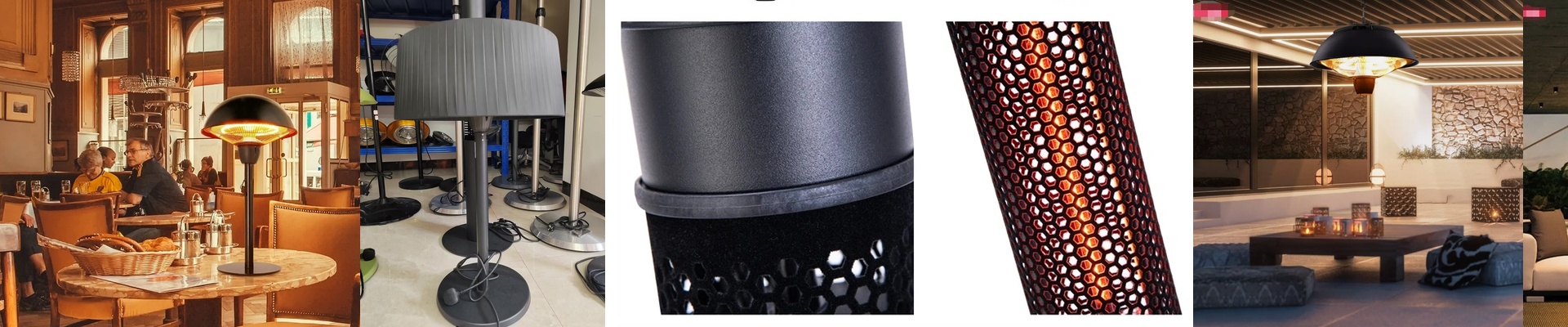
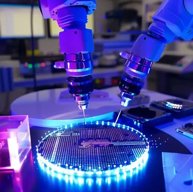
On the fab floor, you learn fast that a 0.5°C drift in photoresist bake temperature can shift a critical dimension by nanometers. Wafer IR heating has to deliver repeatable thermal profiles, shift after shift, without dumping particles into the process or eating up uptime. What matters under the hood We run wafer IR heating modules with short-wave halogen emitters and closed-loop control, holding wafer-level uniformity at ±0.1°C across the bake zone. The response is sub-second, so thermal budgets stay tight and recipe windows don’t drift. The build is cleanroom-ready for Class 1–100, using low-outgassing materials and a path designed to keep particle generation down. Output stays stable over 5,000+ hours, with intensity drift under 5%. Why it plays in lithography In lithography, it comes down to control. Soft bake and hard bake hit target temperature faster and hold it longer, so photoresist thickness, edge bead, and critical dimension uniformity stay predictable. The payoff is tighter distributions, fewer rework lots, and less scrap. Energy use drops, too—the system heats on demand and cools quickly, without overshoot. The module is a drop-in fit for mainstream semiconductor equipment, meeting international equipment interface and control norms. Here is what you need to plan for Installation means matching the tool’s mechanical envelope and electrical interface—double-check connector type, voltage, and coolant compatibility with your platform. Expect a short commissioning run to dial in the thermal profile for your specific wafer stack. Output power density is chosen around the bake step, so very high-power profiles aren’t supported. Plan with that constraint in mind, and the unit will run 24/7 with routine preventive maintenance.